Skip to content

JULY 23, 2026

Accelerating Inference

Accelerating Inference

We’ve raised $300M at a $10.3B valuation, led by Sequoia Capital alongside Andreessen Horowitz, Jane Street, Diffusion, Argo, and SK Hynix. We’re grateful for their support on our journey to Gigawatt-scale.

Our mission is to run the world’s inference. We believe the world’s most powerful models require an entirely new form of computing. Frontier models deserve frontier inference clusters: co-designed chips, packages, PCBs, cold plates, interconnects, and more that push the entire pareto curve on the most demanding workloads.

Today, under 1% of the global population has access to the most advanced AI models. Distributing access will require better technology to deliver more tokens / watt and many Gigawatts worth of compute. Our mission has never been more urgent.

We’ve kicked off fabrication of hundreds of millions of dollars worth of inference clusters. We’ve built a new 10-Megawatt lab fifteen minutes from our office to enable continuous deployment of our first-gen hardware and rapid prototyping of future generations. Production is the product.

We’re excited about bringing our first product to life, and we’re even more excited about what’s to come. If you’d like to work on thousand-chip scale-up domains, in-house SMT lines, and new RL environments for recursive kernel generation, you should join us in accelerating inference.

ETCHEDCOMPANY NEWS

JUNE 30, 2026

Frontier Inference Clusters

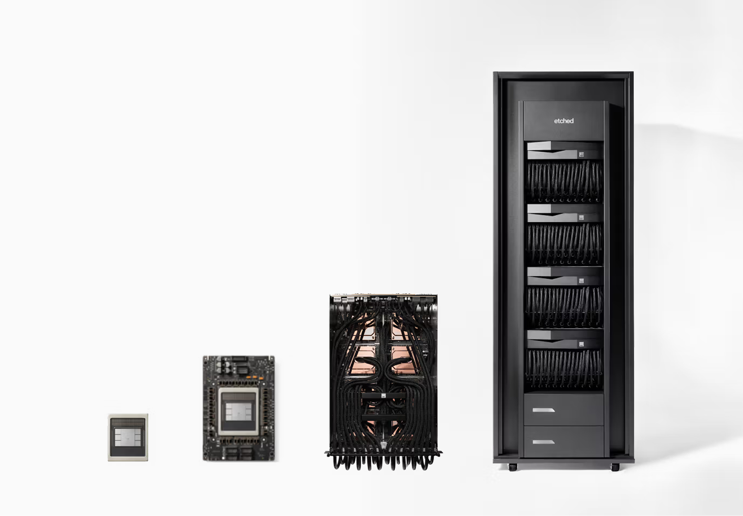
Etched hardware family

We’re building a new category of AI hardware: frontier inference systems.

We co-design chips, racks, software, and manufacturing methods so frontier models can run with best-in-class throughput, latency, cost, and power efficiency for both prefill and decode workloads.

Earlier this year our A0 silicon came back from TSMC N4P, and today we are busy validating our first rack-scale product with customers to fulfill $1B in demand.

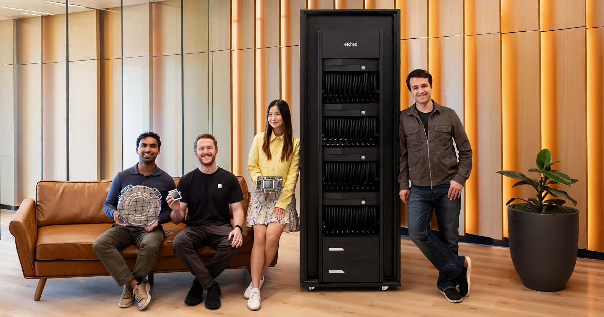
We’re a team of 400+ engineers from NVIDIA, Google TPUs, Broadcom, SK Hynix, TSMC, and more. We’ve raised $800M across four unannounced financings, including a strategic investment from VentureTech Alliance. We’re excited to deepen our partnership with the world’s leading semiconductor manufacturer.
Designing a New Pareto Frontier

Our inference systems are built to push the entire pareto curve on frontier models, including many-trillion-parameter MoEs, long context, and agentic workloads. This required intense co-design, from new chips, packages, PCBs, cold plates, interconnects, and more. Today, we’re sharing two breakthroughs to make this happen:

Low voltage inference (LVI) for high-throughput workloads

Today, AI chips can’t scale FLOPs without thermal throttling. As FLOPs utilization increases, AI chips draw more power and down-regulate clock speed. This often results in sustained inference throughput under half of Peak FLOPs.

We’ve designed a new architecture to run our chip’s math blocks at under half the voltage of most AI chips. This enables multiple times the FLOPs density of AI chips today. We can run trillion-parameter sparse MoEs at 80%+ Peak FLOPs without thermal throttling.

Running LVI requires co-designing the entire cluster from the transistor to the token: new splittable math arrays, circuit techniques, novel tiling and scheduling algorithms, power delivery networks, VRM architectures, advanced packaging, cold plate designs, and more.

Cluster Scale Memory (CSM) for low-latency workloads

Today’s AI chips using HBM can’t achieve SRAM-level decode speeds due to memory subsystem and interconnect bottlenecks. SRAM-only chips have lower FLOPs density and memory capacity, sacrificing throughput.

We created a much lower-latency shared memory pool across our scale-up domain. We use a proprietary ultra-low-latency, high-bandwidth interconnect to enable dramatically faster memory access across chips.

Our HBM/SRAM hybrid design solves both memory capacity and mem2mem latency, enabling high throughput and interactivity simultaneously. CSM improves latency and avoids today’s cost, reliability, yield, thermal, and compute tradeoffs of SRAM-only chips, 3D DRAM chips, or optics.

We’ve made co-design decisions hand-in-hand with leading AI companies, cloud providers, and hyperscalers. We’ve tested racks in representative data center deployments, run terabytes of production traffic patterns through our simulator, and had dozens of engineers live overseas for months to co-design deeply with our supply-chain partners. If this sounds exciting, you should join us.

Getting to Gigawatt Scale

Early customer tests show us achieving SOTA throughput, latency, and power efficiency on inference workloads. We’ll be sharing more updates on our performance and roadmap this summer.

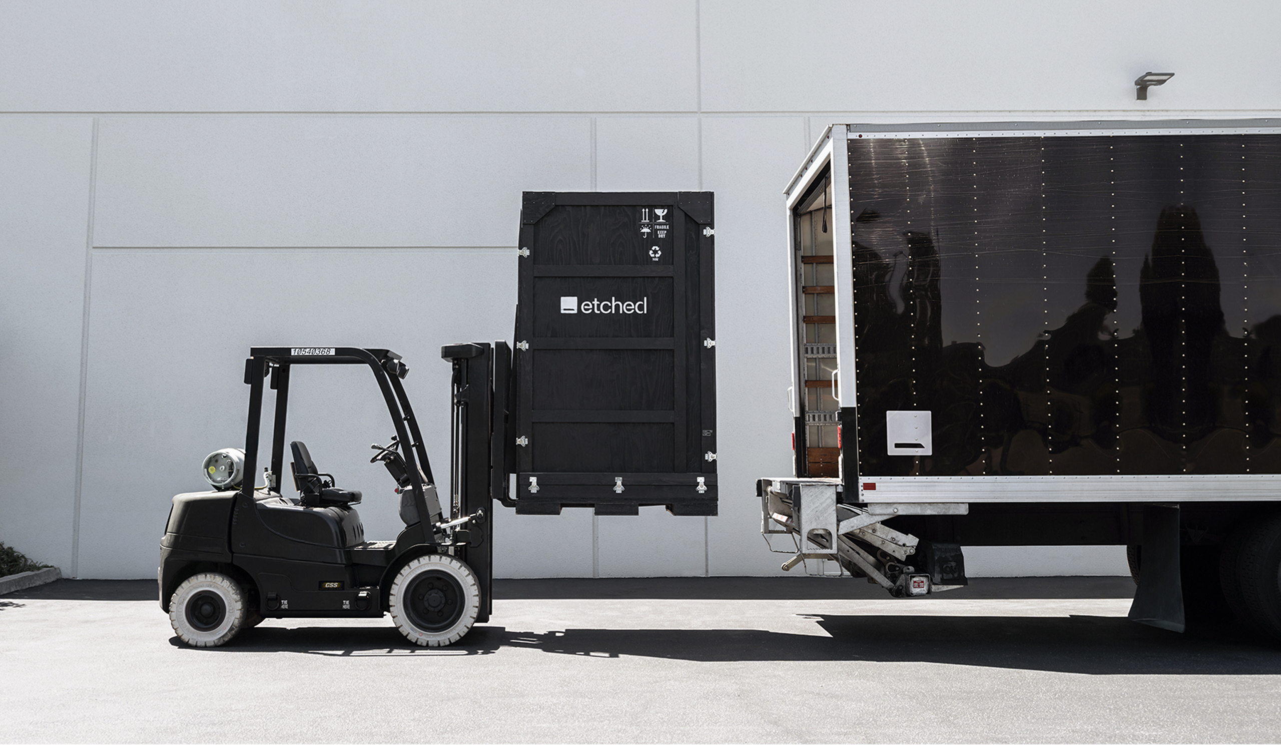
Our first racks ship this summer, and we’ve kicked off production to fulfill over $1B in customer contracts. To enable 24/7 engineering cycles, we’ve opened a Taiwan factory and built a data center, test house, and NPI prototyping lab in our San Jose office.

We are vertically integrated to get to Gigawatt scale as quickly as possible. Math block designers sit next to inference engineers, thermal experts next to GSMs. If this excites you, consider joining us.

ETCHEDCOMPANY NEWS